RF · MIXED-SIGNAL · FPGA · PCB DESIGN
A radio, from the board up.
Arduino made it easy for me to try things in electronics. I wanted something similarly hands-on for radio. The SDRs I could afford were useful, but their hardware was mostly a fixed box; the more flexible RFSoC boards cost far more than I could spend on a personal project.
So I started designing my own receiver. I called it RADIOLAND after a Kraftwerk song I like.
The board is designed for roughly 600 MHz–6 GHz. It has a dual ADC capable of 250 MS/s and an Artix-7 FPGA. I have not tested a built board yet; it is being assembled. Once it works, I want to use it to look at packetized satellite signals, Bluetooth, broadcasts, and eventually the 1.42 GHz hydrogen line.
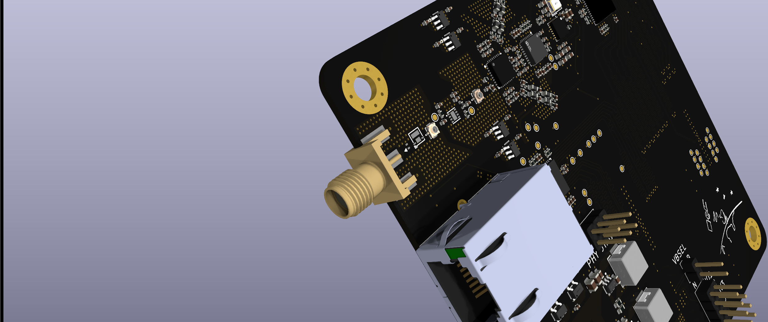
The signal path
The signal comes in through an SMA connector, then goes through protection, a limiter, and a low-noise amplifier before reaching the LTC5586 I/Q demodulator. A MAX2871 PLL/VCO provides the tunable local oscillator. The demodulator gives me differential I and Q baseband signals.
After filtering, an ADS4229 dual 12-bit ADC samples those signals at up to 250 MS/s. Twelve LVDS pairs carry the data to the FPGA. My plan is to do the first processing steps there and eventually send data off the board over Gigabit Ethernet.
Fitting the RF section, ADC, FPGA, and Ethernet onto four layers took a lot of layout work. The RF traces, analog signals, clocks, LVDS pairs, RGMII signals, and separate power rails each had different requirements, and they all had to fit on the same board.
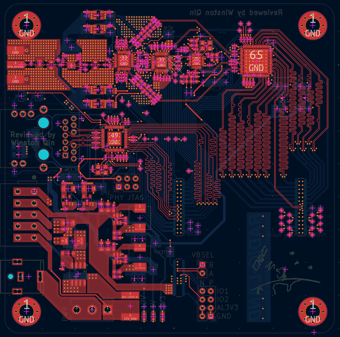
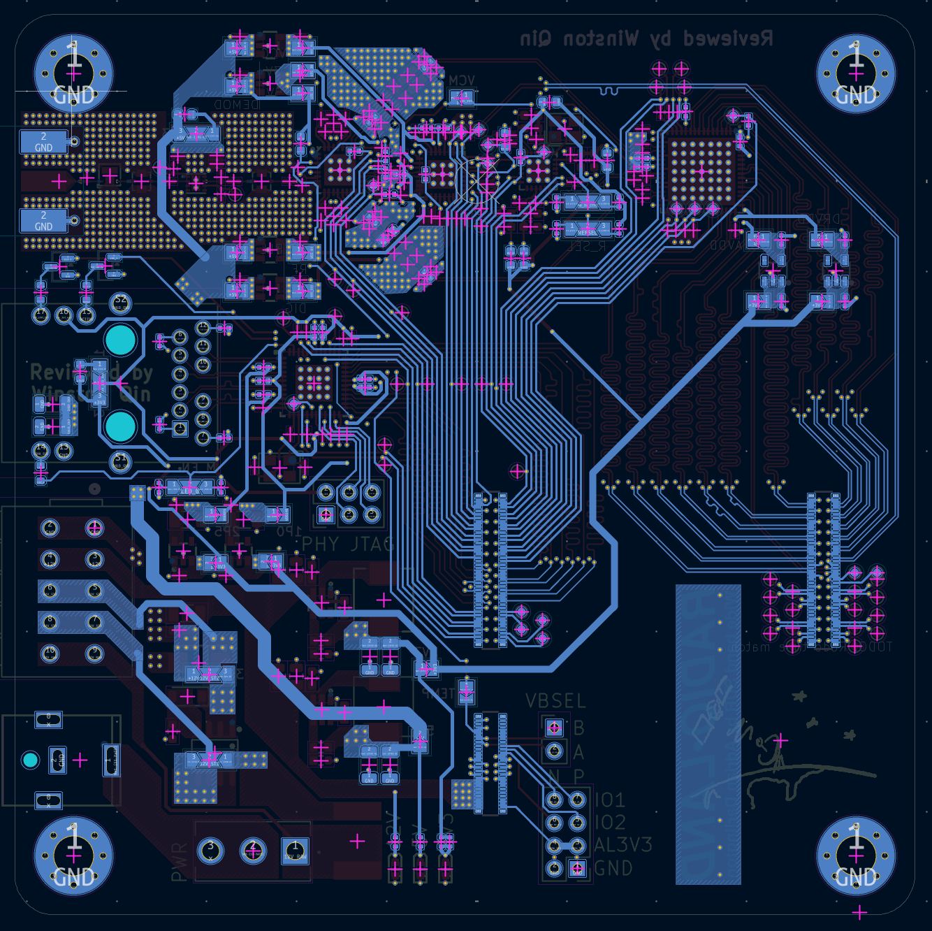
Routing the ADC and Ethernet
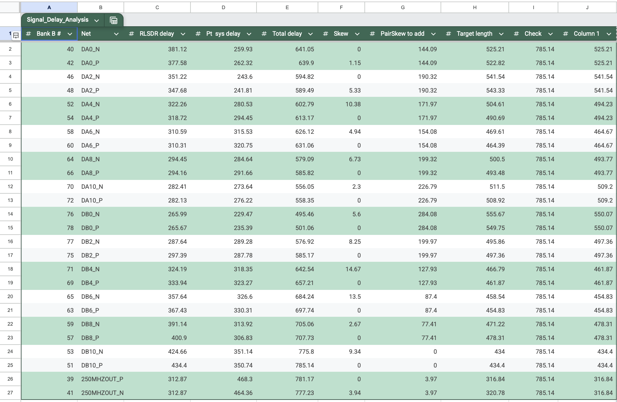
I spent a lot of time on the ADC-to-FPGA interface. Its 12 differential LVDS lanes need to arrive within a tight timing window. I made a spreadsheet for the total delay of each pair, including the PCB traces, vias, and delay through the FPGA module. Equal copper lengths would not necessarily mean equal arrival times, so I used the calculated delays to set the routing targets.
That is why there are so many length-tuning patterns on the board.
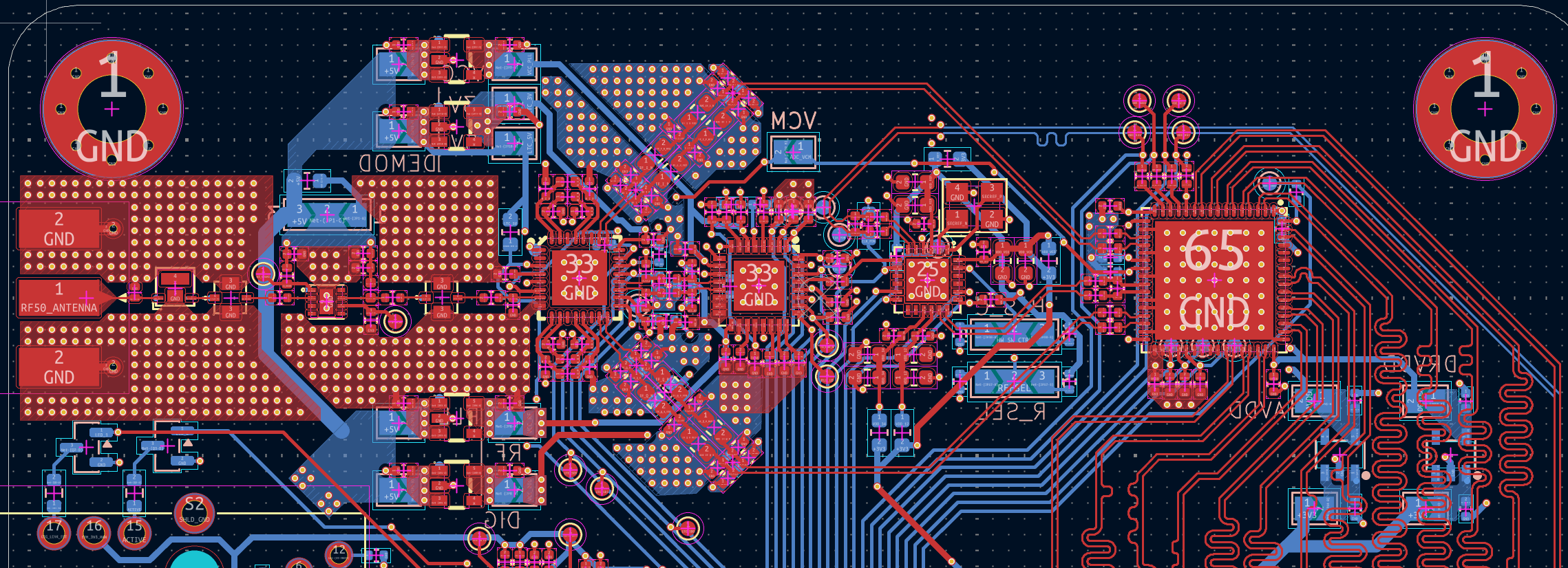
I also caught a pin-planning mistake late. The ADC's LVDS signals need the Alchitry Pt's 2.5 V-capable MV FPGA bank, but my first placement sent them toward the wrong bank. I had to move the FPGA module and redo a large part of the routing. I should have checked the bank assignments before committing to that placement.
I had to settle the board stackup before routing the 50 Ω RF traces and 100 Ω differential pairs. I also spent time checking return paths, clocks, and the power connections.
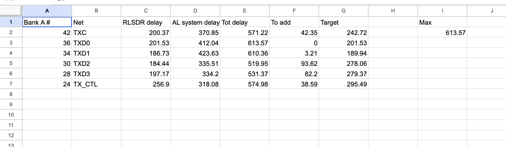
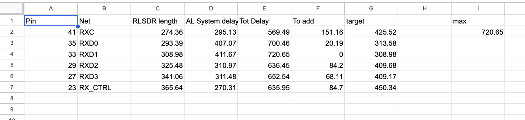
The Ethernet RGMII signals got separate transmit and receive timing sheets. I used the PCB trace delay and delay through the FPGA module to set their routing targets.
Where it stands
The board is 10 × 10 cm, with four layers, controlled-impedance traces, and around 300 components. By my count, I have put more than 300 hours into the design over almost four months. It is with the assembler now, so I do not have RF measurements or captured samples to show yet.
When I get it, I will check the power rails and clocks first, then bring up the PLL, ADC, and Ethernet. After that I can try capturing samples in the FPGA and see how the RF side actually performs. I will update this page with measurements as I get them.